 +44 (0)1592 373601


Clas-SiC enables customers to make the leap from lab to fab, to low/medium production volumes through fast development and prototyping of new SiC devices.
Clas-SiC Solutions
We support customers all the way through development, seeding samples, up to medium volume production, after which we would actively facilitate transfer to a high volume foundry partner.
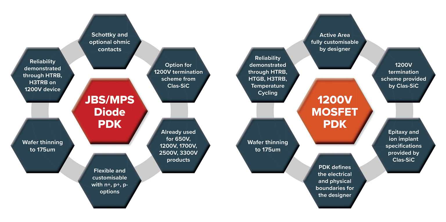
Reliability proven SiC Process Design Kits (PDK’s) are available for planar MOSFETs and JBS/MPS diodes.
Clas-SiC offers not only device processing but also process module solutions as well as individual process capabilities. Our Lochgelly facility achieved the NMI Manufacturing Site of the Year Award in December 2022.
Process Design Kits Released
| 1200V MOSFET Process Design Kit – reliability proven |
| 1700V MOSFET Process Design Kit – reliability proven |
| 3300V MOSFET Process Design Kit – reliability proven |
| JBS/MPS Diode Design Kit – reliability proven |
Process Modules
| Alignment target |
| Implant hard mask |
| Carbon cap implant anneal |
| MOSFET gate dielectric and gate polysilicon |
| Backside ohmic contact |
| Frontside n+ and p+ ohmic contacts |
| Schottky contact |
| MOSFET gate and source contacts |
| Power metal |
| Passivation |
| Backside tri-metal |
| Wafer test |
| Prototype reliability of packaged parts |
| Thinned wafer backside ohmic contact |